- Between every PCIe transmitter (Tx) and receiver (Rx) lane, there’s a series capacitor.
- This capacitor blocks DC voltage but allows high-frequency AC signals (the actual PCIe data) to pass.
👉 In other words:
- DC (static offset) = blocked.
- AC (data transitions) = transmitted.
Why PCIe Uses AC Coupling
-
Common Mode Voltage Independence
- The transmitter may drive its differential pair around one reference level, and the receiver may use a slightly different one.
- With AC coupling, each side can use its own internal reference voltage, since the capacitor blocks any mismatch in DC levels.
-
Noise & Grounding Benefits
- If devices are on different boards, slots, or power domains, their ground/reference voltages may differ.
- AC coupling prevents large DC currents that would otherwise flow due to these mismatches.
-
Signal Integrity
- High-speed PCIe signaling is all about fast transitions (edges).
- Since information is carried in the changes, not the static voltage level, blocking DC does not harm data transmission.
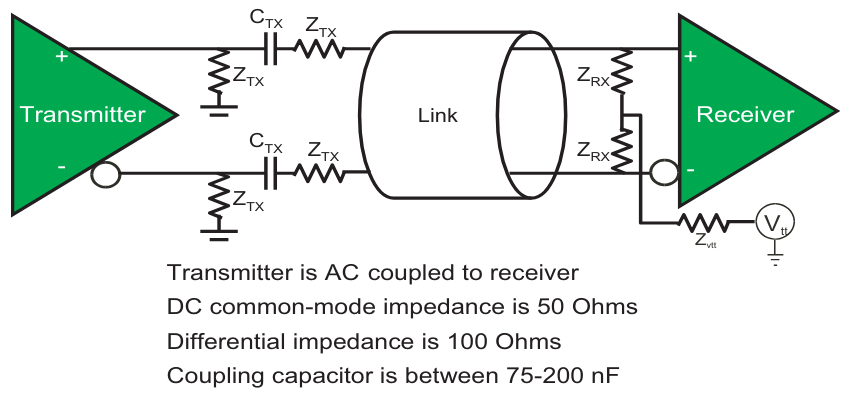
The Physical PCIe Link
-
Differential Pairs:
Each lane = 2 wires (positive + negative). Data is encoded as the difference between them → improves noise immunity. -
AC Coupling Capacitors:
Placed close to the transmitter. Typical values are 75–200 nF. -
Receiver Termination:
The Rx has resistive termination to bias the signal into the correct range after the capacitor.